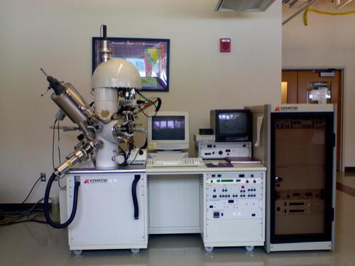
Product Description
X-ray Photoelectron Spectroscopy [ XPS ] Elemental composition of the surface (top 110 nm usually)
Empirical formula of pure materials
Elements that contaminate a surface
Chemical or electronic state of each element in the surface
Uniformity of elemental composition across the top surface (or line profiling or mapping)
Uniformity of elemental composition as a function of ion beam etching (or depth profiling)
Advanced Surface and Thin Film AnalysisOur XPS system delivers high-resolution analysis suitable for a variety of applications, including chemical composition studies and thin film characterization. The monochromatic Al K X-ray source ensures reliable results and reproducibility across semiconductor and materials research, enabling users to confidently interpret surface properties and elemental distributions.
Precision and Automation for Efficient WorkflowsWith multi-sample automation, real-time imaging, and integrated spectral fitting, this XPS instrument streamlines workflows for researchers. Its temperature-controlled sample holder and options for automation improve throughput and consistency when analyzing materials with challenging properties or during repetitive testing cycles.
Robust Safety and Versatile Data ManagementBuilt-in interlocks and emergency power shutdown provide top-tier safety for operators, while the advanced electronics-grade construction ensures durability. Data can be exported in multiple formats, supporting detailed analysis and easy integration with laboratory data management systems.
FAQs of X-ray Photoelectron Spectroscopy- XPS:
Q: How does the XPS system achieve high energy resolution during surface analysis?
A: The XPS instrument employs a hemispherical analyzer and a monochromatic Al K X-ray source, delivering an energy resolution down to 0.5 eV. This configuration ensures precise measurements of binding energy, allowing for detailed chemical state and elemental analysis on sample surfaces.
Q: What types of samples can be examined using this XPS instrument?
A: It is suitable for a broad range of samples, including metals, semiconductors, thin films, and other material science research specimens. The multi-position and temperature-controlled sample holder allows analysis under variable conditions to accommodate diverse sample requirements.
Q: When is ultra-high vacuum required for XPS measurements?
A: Ultra-high vacuum (1x10 mbar) is essential during XPS analysis to prevent surface contamination and interference, ensuring accurate detection of elemental profiles and chemical states. All measurements are performed under these conditions for reliable results.
Q: Where is the XPS system typically installed and operated?
A: Designed as a standard benchtop unit with custom dimensions available, the XPS system is used in research laboratories, university facilities, and industrial R&D centers, particularly within material science and semiconductor sectors. Service is available throughout India.
Q: What is the process for obtaining and analyzing data from the XPS system?
A: The XPS system uses integrated software for spectral fitting and real-time imaging. Users can automate multi-sample measurements, then export data in ASCII, CSV, or proprietary formats for further analysis on computers interfaced via USB, Ethernet, or RS232.
Q: How does this XPS instrument benefit material and semiconductor research?
A: It enables researchers to analyze surface composition, chemical bonding, and film thickness with high spatial and energy resolution, advancing understanding in material innovation, defect inspection, and electronic structure evaluation. Automated features increase efficiency and accuracy.