Product Description
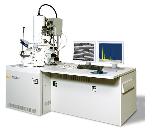
Unlock triumphant precision with our must-have SEM-EDAX Testing servicewhere splendiferous innovation meets inestimable insights. This reduced-cost, advanced solution utilizes Scanning Electron Microscopy (SEM) integrated with Energy Dispersive X-ray Analysis (EDAX) to deliver unmatched high resolution up to 3 nm. Detect elements at the ppm level, with minimal sample preparation required. Compatible with Windows-based software, results are shared as vivid spectra and element maps, stored locally or in the cloud. Try now for rapid, accurate analysis of alloys, metals, composites, and ceramics tailored to your sample size!
Leading-Edge Applications and Features of SEM-EDAX Testing
SEM-EDAX Testing is extensively utilised in research labs, industrial quality control, and forensic material investigations across India. The system showcases high-resolution imaging (up to 3 nm), digital graphical outputs, elemental mapping, and spectra generation. Minimal sample preparation sufficesperfect for powder, solid, film, fiber, and particulates. Windows-compatible software ensures streamlined workflow and real-time data analysis. Robust data storage and USB/Ethernet interfaces enhance its utility in material characterization, failure analysis, and elemental identification projects.
SEM-EDAX Testing Supply, Certifications, and Payments
Our SEM-EDAX Testing service boasts a swift delivery within 2-5 business days and flexible sample customization. With a supply capability ensuring prompt handling of both bulk and single requests, certified results uphold market value and reliability. Sale price transparency underpins our payment options, accommodating bank transfer and standard terms. Each analysis is performed in a certified lab environment, ensuring the highest data accuracy and dependable after-sales support for every client.
FAQs of SEM-EDAX Testing:
Q: How does the SEM-EDAX testing process work?
A: SEM-EDAX testing combines a scanning electron microscope with energy dispersive X-ray analysis to examine and characterize materials at high resolution. Once the sample is prepared (sometimes with a conductive coating), it is scanned to produce digital images and spectra, identifying elemental composition at up to ppm levels.
Q: What samples can be analyzed using this SEM-EDAX service?
A: This service accommodates a versatile range of sample typesincluding powders, solids, films, fibers, and particulatessuiting materials like alloys, metals, composites, and ceramics. The sample size can be customized from microns to centimeters depending on your specific requirements.
Q: When can I expect the delivery of my SEM-EDAX analysis results?
A: Your analytical results will typically be delivered within 2 to 5 business days after sample submission. Output formats include detailed spectra and element maps, provided via secure local or cloud storage options.
Q: Where is SEM-EDAX testing performed and can I access results remotely?
A: SEM-EDAX analysis is conducted in a dedicated, dust-free laboratory environment in India. Results can be accessed remotely thanks to cloud storage and digital delivery options, ensuring your data is both secure and convenient to retrieve.
Q: What are the benefits of choosing this SEM-EDAX testing service?
A: You gain inestimable material insights, accurate elemental determination, and high-resolution imagingall with minimal sample preparation. The service is speedy, supports a wide array of material types, and offers digital, secure data storage and certified analytical accuracy.